- 您现在的位置:买卖IC网 > Sheet目录3882 > PIC16F87T-E/ML (Microchip Technology)IC MCU FLASH 4KX14 EEPROM 28QFN
209
8008H–AVR–04/11
ATtiny48/88
22.4.2
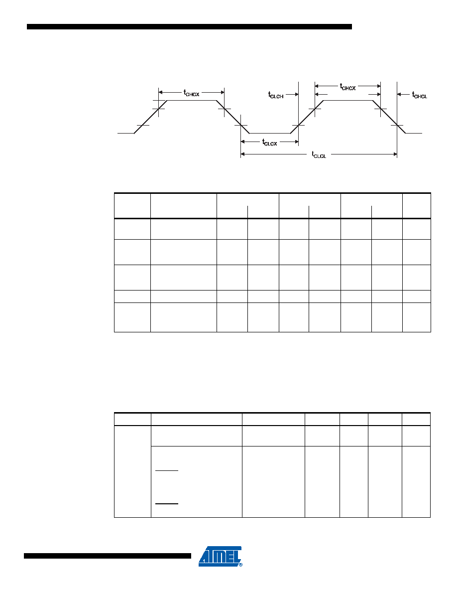
External Clock Drive
Figure 22-2. External Clock Drive Waveforms
Note:
All DC Characteristics contained in this datasheet are based on simulation and characterization of
other AVR microcontrollers manufactured in the same process technology.
22.5
System and Reset Characterizations
Table 22-2.
External Clock Drive
Symbol
Parameter
VCC = 1.8-5.5V
VCC = 2.7-5.5V
VCC = 4.5-5.5V
Units
Min.
Max.
Min.
Max.
Min.
Max.
1/tCLCL
Oscillator
Frequency
02
06
0
12
MHz
tCLCL
Clock Period
250
166
83
ns
tCHCX
High Time
120
80
40
ns
tCLCX
Low Time
120
80
40
ns
tCLCH
Rise Time
2.0
1.6
0.5
s
tCHCL
Fall Time
2.0
1.6
0.5
s
Δt
CLCL
Change in period
from one clock
cycle to the next
22
2
%
VIL1
VIH1
Table 22-3.
Reset, Brown-out, and Internal Voltage Characteristics (1)
Symbol
Parameter
Condition
Min
Typ
Max
Units
VPOT
Power-on Reset Threshold
Voltage (rising)
TA = -40 to +85°C1.5
V
Power-on Reset Threshold
Voltage (falling)(2)
TA = -40 to +85°C1.2
V
VRST
RESET Pin Threshold
Voltage
0.2VCC
0.9VCC
V
tRST
Minimum pulse width on
RESET Pin
VCC = 1.8V
VCC = 3V
VCC = 5V
2000
700
400
ns
发布紧急采购,3分钟左右您将得到回复。
相关PDF资料
PIC16F87-E/ML
IC MCU FLASH 4KX14 EEPROM 28QFN
PIC18LF4320-I/ML
IC MCU FLASH 4KX16 EEPROM 44QFN
PIC16F77T-I/PTG
IC MCU FLASH 8KX14 W/AD 44TQFP
PIC16LF1933-I/SO
IC PIC MCU FLASH 4K 28-SOIC
PIC16C54C-20I/SO
IC MCU OTP 512X12 18SOIC
PIC16LF726-I/SO
IC PIC MCU FLASH 8K 1.8V 28-SOIC
PIC12CE673-10/P
IC MCU OTP 1KX14 A/D&EE 8DIP
PIC16F726-I/SO
IC PIC MCU FLASH 8KX14 28-SOIC
相关代理商/技术参数
PIC16F87T-E/SO
功能描述:8位微控制器 -MCU 20MHz 4K Flash RoHS:否 制造商:Silicon Labs 核心:8051 处理器系列:C8051F39x 数据总线宽度:8 bit 最大时钟频率:50 MHz 程序存储器大小:16 KB 数据 RAM 大小:1 KB 片上 ADC:Yes 工作电源电压:1.8 V to 3.6 V 工作温度范围:- 40 C to + 105 C 封装 / 箱体:QFN-20 安装风格:SMD/SMT
PIC16F87T-E/SS
功能描述:8位微控制器 -MCU 20MHz 4K Flash RoHS:否 制造商:Silicon Labs 核心:8051 处理器系列:C8051F39x 数据总线宽度:8 bit 最大时钟频率:50 MHz 程序存储器大小:16 KB 数据 RAM 大小:1 KB 片上 ADC:Yes 工作电源电压:1.8 V to 3.6 V 工作温度范围:- 40 C to + 105 C 封装 / 箱体:QFN-20 安装风格:SMD/SMT
PIC16F87T-I/ML
功能描述:8位微控制器 -MCU 7KB 368 RAM 16 I/O RoHS:否 制造商:Silicon Labs 核心:8051 处理器系列:C8051F39x 数据总线宽度:8 bit 最大时钟频率:50 MHz 程序存储器大小:16 KB 数据 RAM 大小:1 KB 片上 ADC:Yes 工作电源电压:1.8 V to 3.6 V 工作温度范围:- 40 C to + 105 C 封装 / 箱体:QFN-20 安装风格:SMD/SMT
PIC16F87T-I/SO
功能描述:8位微控制器 -MCU 7KB 368 RAM 16 I/O RoHS:否 制造商:Silicon Labs 核心:8051 处理器系列:C8051F39x 数据总线宽度:8 bit 最大时钟频率:50 MHz 程序存储器大小:16 KB 数据 RAM 大小:1 KB 片上 ADC:Yes 工作电源电压:1.8 V to 3.6 V 工作温度范围:- 40 C to + 105 C 封装 / 箱体:QFN-20 安装风格:SMD/SMT
PIC16F87T-I/SS
功能描述:8位微控制器 -MCU 7KB 368 RAM 16 I/O RoHS:否 制造商:Silicon Labs 核心:8051 处理器系列:C8051F39x 数据总线宽度:8 bit 最大时钟频率:50 MHz 程序存储器大小:16 KB 数据 RAM 大小:1 KB 片上 ADC:Yes 工作电源电压:1.8 V to 3.6 V 工作温度范围:- 40 C to + 105 C 封装 / 箱体:QFN-20 安装风格:SMD/SMT
PIC16F882-E/ML
功能描述:8位微控制器 -MCU 3.5KB Enh FLSH 128 RAM RoHS:否 制造商:Silicon Labs 核心:8051 处理器系列:C8051F39x 数据总线宽度:8 bit 最大时钟频率:50 MHz 程序存储器大小:16 KB 数据 RAM 大小:1 KB 片上 ADC:Yes 工作电源电压:1.8 V to 3.6 V 工作温度范围:- 40 C to + 105 C 封装 / 箱体:QFN-20 安装风格:SMD/SMT
PIC16F882-E/SO
功能描述:8位微控制器 -MCU 3.5KB Enh FLSH 128 RAM RoHS:否 制造商:Silicon Labs 核心:8051 处理器系列:C8051F39x 数据总线宽度:8 bit 最大时钟频率:50 MHz 程序存储器大小:16 KB 数据 RAM 大小:1 KB 片上 ADC:Yes 工作电源电压:1.8 V to 3.6 V 工作温度范围:- 40 C to + 105 C 封装 / 箱体:QFN-20 安装风格:SMD/SMT
PIC16F882-E/SP
功能描述:8位微控制器 -MCU 3.5KB Enh FLSH 128 RAM RoHS:否 制造商:Silicon Labs 核心:8051 处理器系列:C8051F39x 数据总线宽度:8 bit 最大时钟频率:50 MHz 程序存储器大小:16 KB 数据 RAM 大小:1 KB 片上 ADC:Yes 工作电源电压:1.8 V to 3.6 V 工作温度范围:- 40 C to + 105 C 封装 / 箱体:QFN-20 安装风格:SMD/SMT